An EPIc Experience
Tap into more than 25 years of experience in SiC, crystal growth and epitaxy fabricated using proprietary physical vapor transport (PVT) and metal-organic chemical vapor deposition (MOCVD) techniques. Our industry-leading grading structure, introduced in 2014, makes it possible to confidently pinpoint the SiC substrate that optimizes your performance and cost objectives.
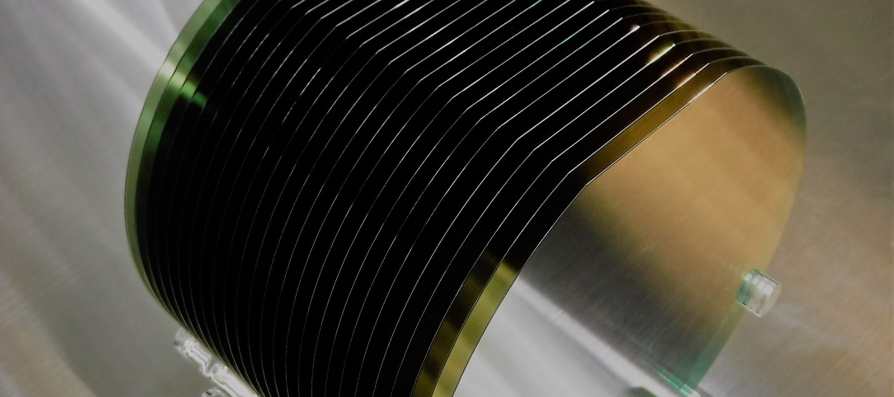
We develop and improve SiC epitaxial wafers, combining one of our 4H single-crystal, 4° off-axis, n-type 150mm or 200mm SiC substrates with an SiC epitaxially grown film for the production of high-performance power devices.
We offer leading edge 150mm SiC homoepitaxial wafers ready to meet the performance and quality needs of device manufacturers. SK siltron css SiC epitaxial wafers feature state of the art thickness and doping uniformity to enable customers to produce best in class SiC devices.
Key Features
- 150 mm wafers
- High quality epitaxy
- State of the art thickness and doping uniformity
- Low defect density
- Leading edge wafer flatness
- Customizable product tolerances to meet specific
customer needs
Grown To Perfection
The epitaxial growth process generates a single-crystal film that is grown in the same orientation as the substrate. We also manufacture the key gas precursor used for epitaxial growth, ensuring a high level of consistent, reliable quality throughout the vertical manufacturing process.
Device manufacturers require precise thickness control, doping (carrier concentration) and defect density to achieve high-yielding power devices from the semiconductor fabrication facility.
Our epitaxial growth process delivers excellence in:
- Excellent thickness control – 25 pt FTIR measurement on each wafer
- Maximum deviation from thickness target for all points measured
- Thickness uniformity from all points measured
- Excellent doping control – 9 pt CV measurement on each wafer
- Maximum deviation from doping target for all points measured
- Doping uniformity from all points measured
- Excellent shape and flatness control – whole wafer interferometer shape inspection
- SBIR / SFQR reported for 10mm x 10mm sites
- Excellent defect control – laser light scattering, defect inspection on each wafer
- Defect detection recipes correlated to device yield
Learn more from our technical PDF on 150 mm SIlicon Carbide Epitaxial Wafers
Material Properties
Note: Please contact your local sales office or SK siltron css technical support before noting final specifications on these products.
150mm SiC epi wafers
| Product Metric (epitaxy 2 to 20µm) | Result |
| Epitaxy doping concentration, cm-3 | |
| Standard epi | 4e+ 15 < Nd < 1e+ 17 |
| Special request | 9e+ 14 < Nd < 2e+ 19 |
| Total of all epilayers target thickness max deviation | ≤10% |
| Total of all epilayers thickness uniformity (sigma/mean) | ≤5% |
| Epilayer net target doping max deviation | ≤15% |
| Epilayer net doping uniformity (sigma/mean) | ≤10% |
| AFM surface roughness – RMS,(1) nm | ≤1 |
| Bow, µm | ±30 |
| Warp, µm | ≤50 |
| TTV, µm | ≤10 |
| SBIR, µm | ≤2 |
Note (n-type, Si-face)
Edge exclusion: thickness, doping and LLS is 5mm EE.
Nominal buffer layer: 1µm @ 1e+18/cm3.
Thickness (measured by FTIR, 25 pts): 2 to 20µm.
Carrier concentration (measured by Hg-CV, 9 pts): 4e+15 to 1e+17/cm3.
Maximum deviation is for all measurement points; percentage reported is calculated from [(Target – Actual)/Target].
Please contact us for information about our 200mm SiC epi wafers
How Can We Help You?
Let us put our materials expertise, application knowledge and processing experience to work for you. To tell us about your performance, design and manufacturing challenges, and learn more about how we can help you, contact us at sales@sksiltron.com.